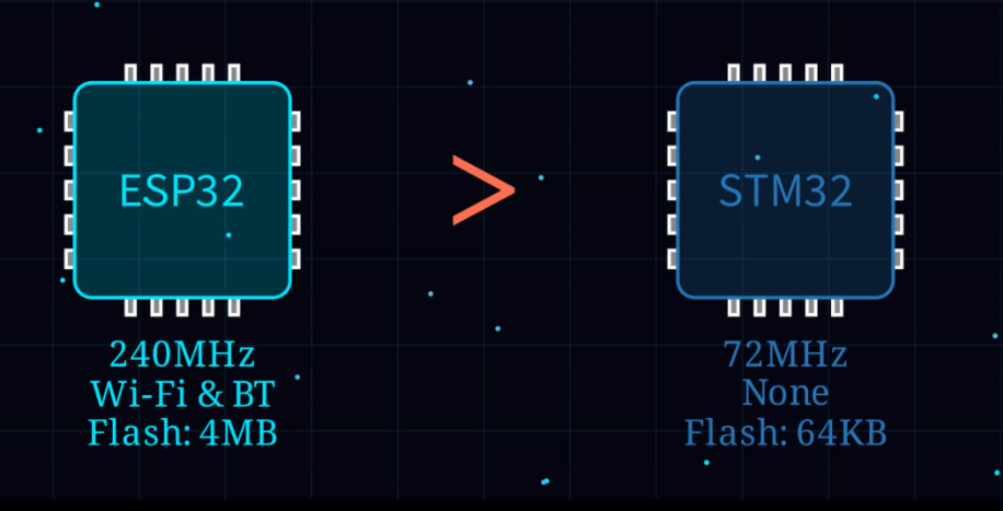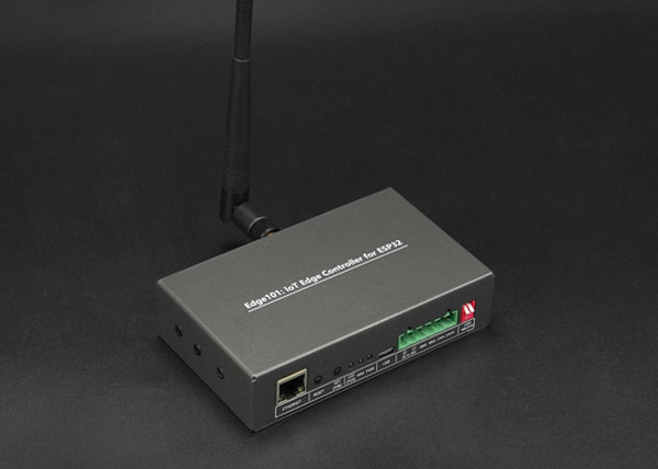
The ESP32 series chips have become the preferred choice for IoT development due to their high cost-effectiveness, rich functionality, and powerful Wi-Fi/BLE wireless communication capabilities. ESP32‑S is an upgraded version released by Espressif, offering significant improvements in RF performance, power consumption control, and system stability.
This article will guide you from scratch, systematically covering the entire PCB design process for ESP32‑S development boards, including:
- Component selection and BOM
- PCB stack-up, signal, and power layout
- RF design and antenna optimization
- Crystal oscillator, USB, and SPI interface routing
- Soldering, assembly, and debugging
- Practical experience and optimization tips
This guide is intended to help hardware enthusiasts, beginners, and even experienced engineers minimize mistakes in PCB design, improve development efficiency, and enhance board performance.
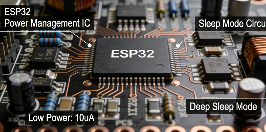
1. Core Objectives of ESP32‑S PCB Design
Before designing the PCB, it is essential to understand the core objectives of an ESP32‑S PCB:
- Stable power system: The instantaneous current during Wi-Fi transmission can reach up to 500mA. Unstable power can cause chip disconnections or resets.
- RF performance optimization: Antenna layout, 50Ω impedance control, and RF area isolation directly affect Wi-Fi and BLE signal quality.
- Signal integrity: High-speed interfaces such as SPI Flash, USB, and PSRAM require shortest-path routing and length-matched differential traces to avoid signal interference.
- Component layout: Crystal oscillators, decoupling capacitors, and sensitive components must be placed close to the chip and away from high-frequency interference.
- Testability and maintainability: Reserve test points, GPIOs, and interfaces for debugging, upgrades, and secondary development.
2. Project Preparation and Component Selection
2.1 Reference Open-Source Projects
Before starting design, it is highly recommended to reference mature open-source projects, such as:
- LCSC EDA open-source ESP32‑S projects
- ESP32 official development board reference designs
When selecting a reference project, pay attention to:
- Project completeness: Must include schematics, PCB layout, BOM, and manufacturing files.
- Component updates: Prefer recently updated projects to avoid obsolete or unstable components.
- Community feedback: Check other users’ comments and modifications to learn practical experience.
Referencing mature projects allows rapid prototyping of the PCB and reduces design risks.
2.2 Core BOM Selection
Below is a typical BOM for an ESP32‑S development board:
| Component Type | Key Parameters | Recommended Model | Selection Reason |
|---|---|---|---|
| Main module | Flash size, package | ESP32‑S‑WROOM‑32U | High-performance Wi-Fi/BLE, QFN package suitable for small boards |
| Power management | Output voltage, current | AMS1117‑3.3/5.0 or DC-DC module | LDO stable, suitable for low-power design |
| USB-to-serial | Driver stability | CH340C | Convenient for programming and serial debugging |
| Decoupling capacitors | High-frequency filtering | 0.1 μF, 1 μF, 10 μF | Reduce power noise and improve stability |
| Peripheral components | LEDs, buttons | 0805 package | Standard package suitable for manual soldering |
Tip: Replacing LDO with a DC-DC converter can significantly reduce power consumption, especially for battery-powered devices.
2.3 Module Package and Antenna Selection
ESP32‑S modules have several common packages:
- Onboard antenna: Suitable for space-limited applications but with shorter range.
- External antenna: Provides longer range and can be expanded with SMA or IPEX connectors.
- Stamp-hole package: Easy for secondary integration, but soldering is more difficult and requires proficient QFN skills.
Note: The antenna area must be designed according to the manufacturer’s recommended keep-out area; otherwise, Wi-Fi signal strength may drop by over 20%.
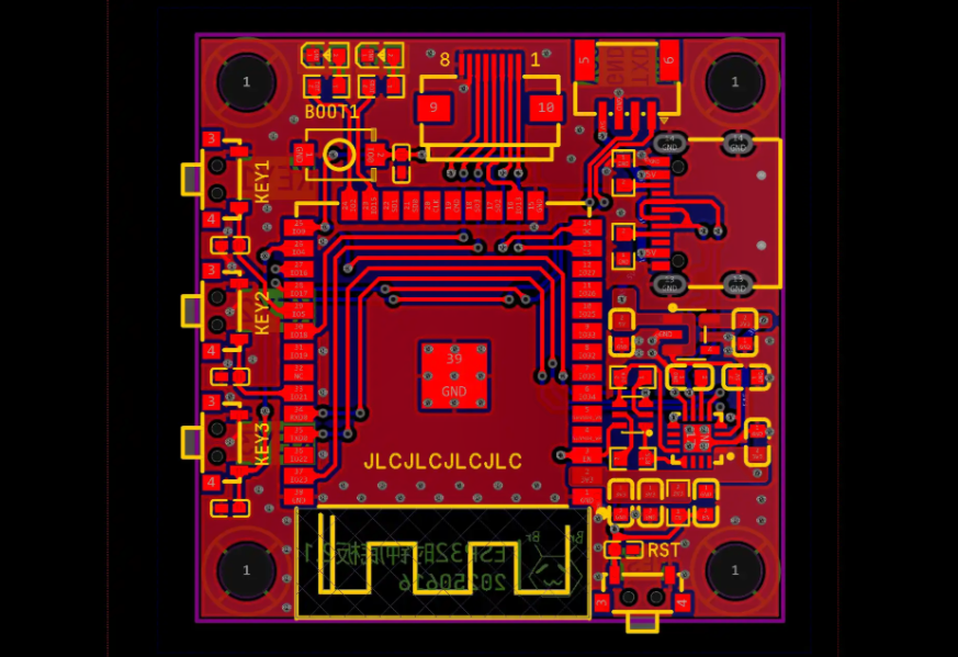
3. PCB Stack-Up and Power Design
-lst-iot")
3.1 PCB Stack-Up Recommendation
The official recommendation is a four-layer PCB:
- L1 Top: Component placement and signal routing
- L2 GND: Continuous ground plane
- L3 POWER: 3.3V/5V power rails
- L4 Bottom: Signal routing and return paths
Advantages:
- Continuous GND plane → reduces EMI
- Stable reference plane for high-frequency signals → improves signal integrity
- Power rails on inner layers → reduces radiation interference
3.2 Power Layout and Decoupling Strategy
- Place input capacitors close to LDO inputs
- Add 0.1 μF high-frequency capacitor for each power pin
- Wide traces for high-current paths ≥ 0.5 mm
- Main power rail filter capacitor ≥ 22 μF
Practical experience: Insufficient 3.3V decoupling can cause Wi-Fi transmission drops or unexpected resets.
3.3 Advanced Optimization
- Use DC-DC converters instead of LDOs to improve efficiency
- Add multiple vias to key power rails to enhance heat dissipation
- Include TVS protection at the power entry to prevent surge damage
4. RF Layout and Antenna Area Design
RF design is a critical factor in the success of an ESP32‑S PCB.
4.1 Antenna Area
- Do not place copper under the antenna.
- Maintain a keep-out area of at least 15 mm around the antenna.
- Avoid placing high-speed digital signals nearby.
- Ensure strict 50Ω impedance to prevent signal reflection.
Practical observation: If copper is mistakenly placed under the antenna, Wi-Fi signal strength can drop by more than 30%.
4.2 RF Trace Routing Tips
- Keep traces as short and straight as possible; minimize bends.
- Avoid crossing layers; maintain continuous reference ground.
- Use a π-type matching network to optimize impedance.
- Place high-frequency capacitors close to the module pins.
4.3 High-Frequency Signal Isolation
- Separate digital and RF signals into different regions.
- Keep the ground copper as continuous as possible.
- Avoid routing high-frequency signals parallel to the crystal oscillator or SPI Flash.
5. Crystal Oscillator Layout and Sensitive Components
- Place the crystal oscillator close to the module, away from high-frequency interference.
- Lay continuous ground copper under the crystal.
- Arrange surrounding capacitors symmetrically.
Tip: Interference with the crystal oscillator can cause Wi-Fi packet loss and clock jitter.
6. High-Speed Interface Layout (SPI / USB)
6.1 SPI Flash / PSRAM
- Keep traces as short as possible.
- Maintain continuous ground planes and minimize vias.
- Surround CLK and DATA lines with ground copper to reduce crosstalk.
6.2 USB
- D+/D- differential impedance: 90Ω
- Use length-matched traces.
- Minimize vias.
- Keep a continuous ground plane as a reference.
-lst-iot")
7. Soldering and Assembly Practices
7.1 Tools and Materials
- Temperature-controlled soldering station (300–350°C)
- 0.5 mm silver-containing lead-free solder
- Flux, solder wick
- Magnifying glass or microscope
7.2 Soldering Process
- Clean the PCB pads and apply flux.
- Align the module using tweezers.
- Solder diagonal pins first to fix position, then solder the remaining pins.
- Inspect for bridges or cold solder joints under magnification.
Note: The bottom pads of QFN modules are difficult to inspect; X-ray or microscope inspection is recommended.
8. Functional Testing and Debugging
8.1 Power and Static Tests
- Ensure stable 3.3V output.
- Verify static current < 10 mA.
8.2 Communication Tests
- Confirm USB-to-serial driver works correctly.
- Check AT command responsiveness.
8.3 Peripheral Tests
- GPIO input and output functionality.
- LED and button operation.
- Wi-Fi and BLE scanning.
8.4 Common Problems and Solutions
| Issue | Possible Cause | Solution |
|---|---|---|
| No power | Power reversed | Check polarity and replace components |
| USB not recognized | Differential impedance mismatch | Adjust D+/D- trace routing |
| Weak Wi-Fi signal | Antenna layout error | Maintain antenna keep-out area |
| Unable to program | GPIO0 not pulled low | Adjust boot circuit |
9. Final PCB Checklist Before Release
- Four-layer design with continuous GND plane
- Adequate power filtering and decoupling
- Clear antenna area with 50Ω impedance
- Correct crystal oscillator placement
- Differential impedance optimized for high-speed interfaces
- Boot, EN, and GPIO0 circuits correct
- Length-matched USB and serial traces
Recommendation: Use simulation tools to verify impedance and signal integrity before release to further reduce risk.
10. Advanced Optimization Suggestions
- Power efficiency: Use DC-DC converters instead of LDOs.
- EMC improvements: Apply shielding and filtering networks.
- Mechanical structure optimization: Add mounting holes, board edge clearance, and extra test points.
- Future-proofing: Plan secondary integration interfaces in advance.
Summary
ESP32‑S PCB design is not just “drawing traces”; it is a comprehensive engineering task encompassing power integrity, RF performance, and signal integrity. By following official guidelines combined with industry best practices, you can design a stable, high-performance, and reliable development board.
This guide can serve as a professional technical reference, suitable for publishing as a high-quality blog article or for team technical documentation and design standards.