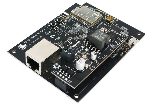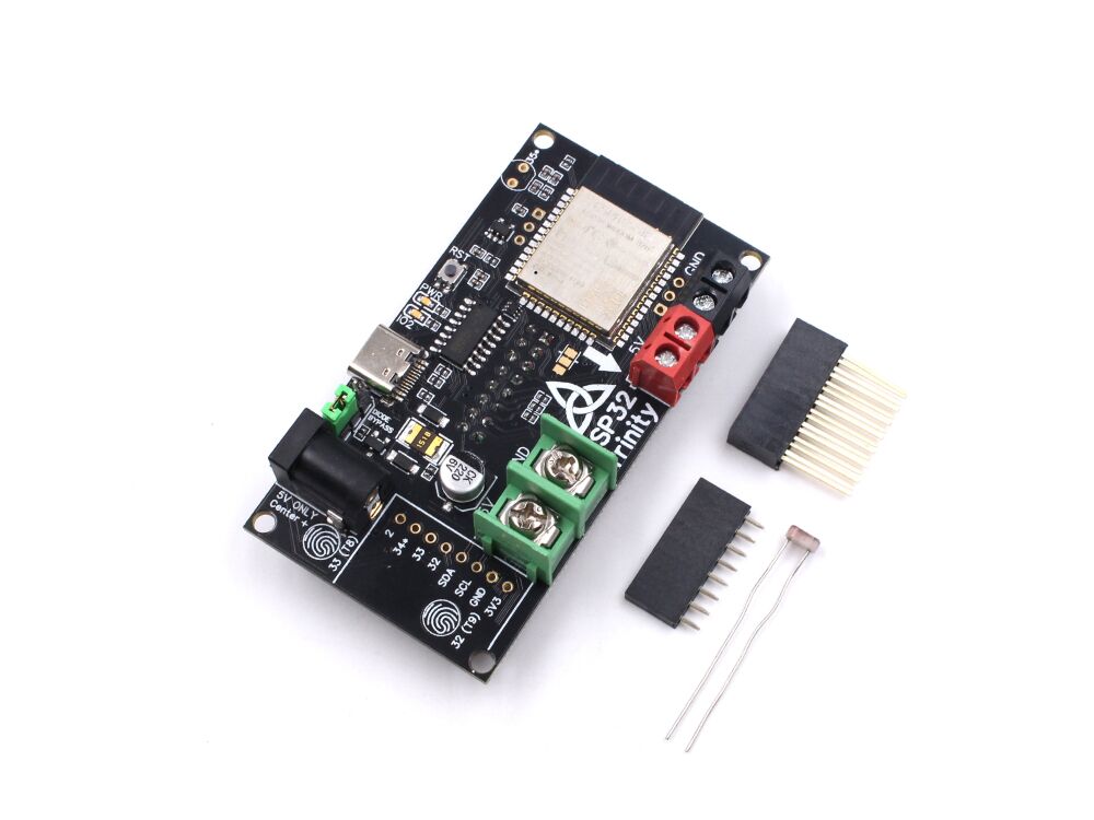
What is ESP32 PCB Design?
ESP32 PCB design refers to the development of circuit boards that support the ESP32 chip in embedded systems. It involves combining hardware design, RF engineering, and power management into a single optimized layout.
Unlike standard microcontroller boards, ESP32 designs must handle:
- High-frequency RF signals (Wi-Fi & Bluetooth)
- Power fluctuations during transmission
- Electromagnetic interference (EMI)
- Signal integrity across multiple interfaces
This makes ESP32 PCB design significantly more complex than traditional MCU layouts.
ESP32 vs Other MCU PCB Design (Key Differences)
| Feature | Traditional MCU PCB | ESP32 PCB Design |
|---|---|---|
| Wireless | External modules | Built-in Wi-Fi & Bluetooth |
| RF Design | Not required | Critical |
| Power Stability | Moderate | Highly sensitive |
| Layout Complexity | Medium | High |
| EMI Consideration | Basic | Advanced |
Conclusion: ESP32 requires RF-aware PCB design and stricter layout control.
Key Components in ESP32 PCB Design
A high-performance ESP32 PCB relies on the correct integration of several subsystems:
1. Power Supply & Decoupling Design
- Stable 3.3V voltage regulation
- Use of bulk capacitors + high-frequency decoupling capacitors
- Placement close to ESP32 power pins
Best Practice:
Use a combination of:
- 10µF (bulk)
- 0.1µF (high-frequency)
Poor power design = unstable Wi-Fi + random resets
2. Antenna & RF Layout Design
ESP32 performance heavily depends on antenna design:
- Keep antenna area free of copper and components
- Maintain controlled impedance (typically 50Ω)
- Avoid ground planes under antenna
Critical Rule:
Never place metal, vias, or traces under the antenna zone.
3. Sensors & Peripheral Integration
ESP32 supports multiple interfaces:
- I2C (low-speed communication)
- SPI (high-speed devices)
- UART (debug & modules)
Design Tips:
- Separate analog and digital signals
- Keep sensor traces short
- Use proper grounding
ESP32 PCB Design Workflow (Step-by-Step)
A structured workflow ensures reliable PCB results:
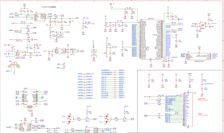
Step 1: Schematic Design
- Define circuit connections
- Choose ESP32 module or chip
Step 2: Component Placement
- Place ESP32 centrally
- Keep power components nearby
- Position antenna at board edge
Step 3: PCB Routing
Focus on three priorities:
- Power traces → short and wide
- RF traces → controlled impedance
- Signal traces → avoid crossing and loops
Step 4: Ground Plane Design
- Use continuous ground plane
- Avoid splits under critical signals
- Ensure low return path impedance
Step 5: DRC & Prototyping
- Run design rule checks
- Manufacture prototype
- Validate RF and power performance
Common Challenges in ESP32 PCB Design
1. RF Signal Interference
- Caused by poor antenna placement
- Results in weak Wi-Fi signal
2. Power Instability
- Voltage dips during transmission
- Leads to system resets
3. EMI/EMC Issues
- Noise coupling between circuits
- Affects overall system reliability
4. Poor Layout Decisions
- Long traces
- Improper grounding
- Mixed signal routing
ESP32 PCB Design Best Practices (Checklist)
Use this checklist before finalizing your design:
✔ Power Design
- Place decoupling capacitors close to VCC
- Use solid ground plane
✔ RF Layout
- Keep antenna at board edge
- Avoid interference sources
✔ Routing
- Keep traces short and direct
- Avoid sharp angles (use 45° routing)
✔ Grounding
- Continuous ground plane
- No fragmented return paths
Quick Design Summary
| Design Area | Key Rule |
|---|---|
| Power | Strong decoupling |
| RF | Clear antenna zone |
| Routing | Short & clean |
| Ground | Solid plane |
Advanced ESP32 PCB Design Considerations
To achieve professional-level designs:
- Use 4-layer PCB for better EMI control
- Separate RF and digital sections
- Apply EMI shielding techniques
- Optimize impedance matching
These techniques are essential for industrial and commercial products.
FAQ: ESP32 PCB DesignWhat is the best layout for ESP32?
The best layout places the ESP32 centrally, keeps power components close, and positions the antenna at the edge with no interference.
How do I improve ESP32 Wi-Fi performance?
- Optimize antenna placement
- Use proper impedance matching
- Reduce RF interference
How to reduce ESP32 power consumption on PCB?
- Use efficient regulators (DC-DC)
- Optimize sleep modes
- Minimize leakage paths
What is the biggest mistake in ESP32 PCB design?
Poor antenna layout and weak power design are the most common causes of failure.
Final Thoughts
ESP32 PCB design requires a balance between RF performance, power integrity, and layout optimization. Engineers who follow structured design practices and apply best practices can significantly improve product reliability and wireless performance.